Xbox ONE has a 5 billion transistor GPU

  • 124 results
  • 1
  • 2
  • 3

This topic is locked from further discussion.

Avatar image for Krelian-co
Krelian-co

13274

Forum Posts

0

Wiki Points

0

Followers

Reviews: 1

User Lists: 0

#101 Krelian-co
Member since 2006 • 13274 Posts

[QUOTE="lostrib"]

[QUOTE="CallOfDutyRulez"]

Is the tech info too compelx for your small hermit brain?

The xbox ONE is stronger than the strongest gaming PC on the market.

CallOfDutyRulez

no

it's more that you apparently pulled it from a livejournal

So, how does it feel that you paid $10,000 for a multiplat machine with worse graphics than a $500 xbox ONE?

i paid $20.000 for mine, nasa sold it to me directly.

Avatar image for Krelian-co
Krelian-co

13274

Forum Posts

0

Wiki Points

0

Followers

Reviews: 1

User Lists: 0

#102 Krelian-co
Member since 2006 • 13274 Posts

[QUOTE="clyde46"]And? My GTX 580 had 3 billion and its now two gens behind.CallOfDutyRulez

Older architecture... The xbox ONE is clearly 5 years ahead of the best gaming PCs.

trolling has to be more subtle.

you-went-full-retard-never-go-full-retar

Avatar image for Grey_Eyed_Elf
Grey_Eyed_Elf

7971

Forum Posts

0

Wiki Points

0

Followers

Reviews: 0

User Lists: 0

#103 Grey_Eyed_Elf
Member since 2011 • 7971 Posts

[QUOTE="CallOfDutyRulez"]

[QUOTE="lostrib"]

no

it's more that you apparently pulled it from a livejournal

Krelian-co

So, how does it feel that you paid $10,000 for a multiplat machine with worse graphics than a $500 xbox ONE?

i paid $20.000 for mine, nasa sold it to me directly.

20,000 is not enough... remember you need to raid 0 PCIE SSD drives to reach the speeds of the overall performance of the X1 and your ram needs to be DDR4 at the very least.
Avatar image for Krelian-co
Krelian-co

13274

Forum Posts

0

Wiki Points

0

Followers

Reviews: 1

User Lists: 0

#104 Krelian-co
Member since 2006 • 13274 Posts

[QUOTE="Krelian-co"]

[QUOTE="CallOfDutyRulez"]

So, how does it feel that you paid $10,000 for a multiplat machine with worse graphics than a $500 xbox ONE?

Grey_Eyed_Elf

i paid $20.000 for mine, nasa sold it to me directly.

20,000 is not enough... remember you need to raid 0 PCIE SSD drives to reach the speeds of the overall performance of the X1 and your ram needs to be DDR4 at the very least.

i present to you my gamin room, i ordered when i found out the kind of power ps4 and xbone would have, i hope i can run games like consoles do.

super-computer-room.jpg

Avatar image for ronvalencia
ronvalencia

29612

Forum Posts

0

Wiki Points

0

Followers

Reviews: 1

User Lists: 0

#105 ronvalencia
Member since 2008 • 29612 Posts

[QUOTE="ronvalencia"]

[QUOTE="tormentos"]

Still remember those who claimed that this would be the spec..:lol:

Even Ronvalencia tagged Volcanic Island once to the xbox one...:lol:

the tormentos

:lol:

Based on somebody's rumor. All I stated is technology to reach that goal at reasonable cost (which is based on historical die size) i.e. 20 nm process tech would be required.

I didn't say X1 will actually have AMD VI.

You keep missing the word IF

Oh please you rided Volcanic Island with the xbox one...:lol: because for you MS had money to burn and everything was possible...:lol:

http://au.gamespot.com/forums/topic/29393862/specs-for-nextbox-leaked-more-powerful-than-ps4?page=12

Xbox 360's total chip size from http://www.anandtech.com/show/2682/4

1st gen:

- CPU: 176 mm^2

- GPU: 182 mm^2

- eDRAM: 80 mm^2

Total chip size: 438 mm^2

-------------------

2nd gen:

- CPU: 135 mm^2

- GPU: 156 mm^2

- eDRAM: 64 mm^2

Total chip size: 355 mm^2

--------------------

TSMC's 20nm process tech makes the TC'srumor possible. :lol:

---------------

Possibilities != actual.You can't handle shades of grey.

http://www.merriam-webster.com/dictionary/possible

Definition of POSSIBLE

1

a : being within the limits of ability, capacity, or realization

b : being what may be conceived, be done, or occur according to nature, custom, or manners

2

a : being something that may or may not occur :lol:

b : being something that may or may not be true or actual :lol:

3

: having an indicated potential

The above X1 estimate the similar to my PS4 and it's still up to MS to select the 20nm part.

HD 7850's die size already smaller than 1st gen NVIDIA RSX.

---

1st gen NVIDIA RSX = 258 mm^2

1st gen IBM CELL = 230 mm^2

Total die size: 488 mm^2

---

Option 1

AMD Radeon HD 7850 (16 CU GpGPU) = 212 mm^2

AMD Trinity (6 CU IGP) = 246 mm^2

Total die size: 458 mm^2

---

Option 2

Semi-custom AMD Trinity (quad core PileDriver) with Radeon HD 7850 = ~335 mm^2

Quad core PileDriver = ~50 watts (with 4th core for yield issues).

Radeon HD 7850 = 130 watts (16 CUs operational, with 4 CUs disabled for yeild issues).

Total: 180 watts.

---

Option 3

Semi-custom AMD Jaguar with 8 cores with Radeon HD 7850

AMD Jaguar core: 3.1 mm^2 + 2.1 mm^2 L2 cache = 5.2 mm^2 x 8 cores = 41.6 mm^2 (28nm process tech)

AMD Radeon HD 7850 (16 CU GpGPU) = 212 mm^2 (28nm process tech)

Total : 253.6 mm^2, ~150 watts. ---

Based on 1st gen PS3, power consumption can be around 209 watts (e.g. FF13) i.e. PS3 used 380 watt power supply. Option 2 is possible for PS4.

If there was a rumour that Sony updates to VI, I'll do an estimate for PS4. AMD VI would be software compatible with PS4's software ecosystem.

Avatar image for ronvalencia
ronvalencia

29612

Forum Posts

0

Wiki Points

0

Followers

Reviews: 1

User Lists: 0

#106 ronvalencia
Member since 2008 • 29612 Posts

http://misterxmedia.livejournal.com/

"Xbox One will have 8GB of RAM + 4 GB of Stacked new type of RAM for a total of 12GB as it was spotted on several dev kits leaks."

"mistercteam: 2x7970 GCN1.0 is the devkit RAW power, GCN 2.0 is much much efficient design that's the point
look at the 2560 ALU focus on that
then add GCN 2.0
add esRAM
add move engine
add Custom CPU"

"on raw performance it is between 7970 and 2x7970
see it is same like parasite or misterx insider
it is about 4.8 TF RAW"

"mistercteam: XB1 GPU certainly will be > 768 ALU , in GCN Term

Mister X insider said 2304 ALU, And later on 2x8970m = 2560 ALU
Parasite76 , 3 times , so about same as 2560/2304 ALU

The GCN 2.0 at 28nm , as Sushi Guy said, it is > 2800 ALU
the 20nm GCN 2.0 is > 3072 ALU

So it is safe to specualter XB1 GPU will be 2304 -2560 (PC AMD top end will be 2880 or more, the 20nm will be 3072 or more),
but the key aspect is XB1 is 2.0+ it is adding more efficient desgin by adding SRAM to GCN 2.0, also it is close environment, and the OS is more foucused for console performance

So when AMD release the GCN 2.0 with improved design
XB1 is at least already 1 step design same as XBox 360 1 step more advanced

The Die size on wired photo certainly > 500mm^2
the rumored 9950 2304 also have 5 Billion T

Microsofts PR department
> 5 BillionT
http://www.extremetech.com/gaming/156453-xbox-one-more-like-xbox-none-ms-blew-the-xbox-720-reveal-on-every-conceivable-level/2
"more than 5 billion transistors "


If they have to disclose it at Hotchip
it must be some breakthrough design , Hotchip is a high calibre
event

Also The Timing is so perfect aligned
Gamescom
Hotchip
AMD APU 13

This year We Will got GCN 2.0 GPU
XB one is GCN 2.0+ (GCN 2 + Move engine + SRAM)

...

mistercteam: to sum it up, please read 1-4 post above before this, to read all link, pdf and others, also live streaming from Doug, director of MS research & CLoud.
Live streaming (MS research) scheduled at 15 July 2013, also featuring keynote from Bill Gates.

Now back to T3 core (improvement from edge/trips)
this is 32 core of edge/trips performace
from wiki and pdf

" 32 chips interconnected, approaching 500 GFLOPS"

now imagine 192 VSP (12 shader core) = 768 operation)

192 = 6 x 32 = 6 x 0.5TF = 3 TF at 1 Ghz, at 800 Mhz = 2.4 TF

imagine we up the shader core like rumored to be 24 SC at least.
24 SC = 384 = 12 x 32core = 12 x 0.5 TF = 6 TF = 4.9 TF at 800 Mhz (like parasite said)
how it is somehow fit so much

also that based on edge/trips performance
what about MS own T3 core, it is 50% more than trips/edge
so 24 SC = 384 T3 core = 4.9 x 1.5 = > 7 TF (wow)(real close box , performance
after they can utilize it, on base spec it is 4.9 TF at 24 shader core

no wonder it is called gfx core or shader core not compute unit
no wonder MS targetted at only 100-180W low clock

this thinng is new architecture
in the future they can pass xx TF easily just using 1.2 Ghz clock

they just choose AMD as partner to design it
the basic edge/trips are MS-Intel-IBM-SUN research

MS takes it further to develop it as real CPU for gaming use
with the help of IBM-AMD
remember MS have capability to write SDK, kernel, Framework
to make it happen

Like Rob Shearer (Eric Team) said, only 2 things that drive computing forward:
Server/High performance Computing & Gaming COnsole

*) also why they have to use 1x7970 or 2x7970 now rather make sense
*) also how that Edge/trips research pdf are same year as MS leaked Xbox next roadmap 2010

....

CallOfDutyRulez

5 billion - 1.6 billion (T6 ESRAM) = 3.4 billion transistors.

No 7970/8970 (4.3 billion transistors) class GPU for X1.

Avatar image for tormentos
tormentos

33793

Forum Posts

0

Wiki Points

0

Followers

Reviews: 0

User Lists: 0

#107 tormentos
Member since 2003 • 33793 Posts

[QUOTE="tormentos"]

[QUOTE="ronvalencia"]

:lol:

Based on somebody's rumor. All I stated is technology to reach that goal at reasonable cost (which is based on historical die size) i.e. 20 nm process tech would be required.

I didn't say X1 will actually have AMD VI.


You keep missing the word IF

ronvalencia


Oh please you rided Volcanic Island with the xbox one...:lol: because for you MS had money to burn and everything was possible...:lol:


http://au.gamespot.com/forums/topic/29393862/specs-for-nextbox-leaked-more-powerful-than-ps4?page=12


Xbox 360's total chip size from http://www.anandtech.com/show/2682/4

1st gen:

- CPU: 176 mm^2

- GPU: 182 mm^2

- eDRAM: 80 mm^2

Total chip size: 438 mm^2

-------------------


2nd gen:

- CPU: 135 mm^2

- GPU: 156 mm^2

- eDRAM: 64 mm^2

Total chip size: 355 mm^2

--------------------

TSMC's 20nm process tech makes the TC'srumor possible. :lol:


---------------

Possibilities != actual.You can't handle shades of grey.

http://www.merriam-webster.com/dictionary/possible


Definition of POSSIBLE


1

a : being within the limits of ability, capacity, or realization

b : being what may be conceived, be done, or occur according to nature, custom, or manners

2

a : being something that may or may not occur :lol:

b : being something that may or may not be true or actual :lol:

3

: having an indicated potential


The above X1 estimate the similar to my PS4 and it's still up to MS to select the 20nm part.


HD 7850's die size already smaller than 1st gen NVIDIA RSX.

---

1st gen NVIDIA RSX = 258 mm^2

1st gen IBM CELL = 230 mm^2

Total die size: 488 mm^2


---

Option 1

AMD Radeon HD 7850 (16 CU GpGPU) = 212 mm^2

AMD Trinity (6 CU IGP) = 246 mm^2

Total die size: 458 mm^2

---

Option 2

Semi-custom AMD Trinity (quad core PileDriver) with Radeon HD 7850 = ~335 mm^2

Quad core PileDriver = ~50 watts (with 4th core for yield issues).

Radeon HD 7850 = 130 watts (16 CUs operational, with 4 CUs disabled for yeild issues).

Total: 180 watts.

---

Option 3

Semi-custom AMD Jaguar with 8 cores with Radeon HD 7850

AMD Jaguar core: 3.1 mm^2 + 2.1 mm^2 L2 cache = 5.2 mm^2 x 8 cores = 41.6 mm^2 (28nm process tech)

AMD Radeon HD 7850 (16 CU GpGPU) = 212 mm^2 (28nm process tech)

Total : 253.6 mm^2, ~150 watts. ---

Based on 1st gen PS3, power consumption can be around 209 watts (e.g. FF13) i.e. PS3 used 380 watt power supply. Option 2 is possible for PS4.


See you still belive it even when every damn source say it was GCN and not GCN 2..


Nothing further to prove..:lol:

Avatar image for ronvalencia
ronvalencia

29612

Forum Posts

0

Wiki Points

0

Followers

Reviews: 1

User Lists: 0

#108 ronvalencia
Member since 2008 • 29612 Posts

[QUOTE="ronvalencia"]

[QUOTE="tormentos"]

Oh please you rided Volcanic Island with the xbox one...:lol: because for you MS had money to burn and everything was possible...:lol:

tormentos

http://au.gamespot.com/forums/topic/29393862/specs-for-nextbox-leaked-more-powerful-than-ps4?page=12

Xbox 360's total chip size from http://www.anandtech.com/show/2682/4

1st gen:

- CPU: 176 mm^2

- GPU: 182 mm^2

- eDRAM: 80 mm^2

Total chip size: 438 mm^2

-------------------

2nd gen:

- CPU: 135 mm^2

- GPU: 156 mm^2

- eDRAM: 64 mm^2

Total chip size: 355 mm^2

--------------------

TSMC's 20nm process tech makes the TC'srumor possible. :lol:

---------------

Possibilities != actual.You can't handle shades of grey.

http://www.merriam-webster.com/dictionary/possible

Definition of POSSIBLE

1

a : being within the limits of ability, capacity, or realization

b : being what may be conceived, be done, or occur according to nature, custom, or manners

2

a : being something that may or may not occur :lol:

b : being something that may or may not be true or actual :lol:

3

: having an indicated potential

The above X1 estimate the similar to my PS4 and it's still up to MS to select the 20nm part.

HD 7850's die size already smaller than 1st gen NVIDIA RSX.

---

1st gen NVIDIA RSX = 258 mm^2

1st gen IBM CELL = 230 mm^2

Total die size: 488 mm^2

---

Option 1

AMD Radeon HD 7850 (16 CU GpGPU) = 212 mm^2

AMD Trinity (6 CU IGP) = 246 mm^2

Total die size: 458 mm^2

---

Option 2

Semi-custom AMD Trinity (quad core PileDriver) with Radeon HD 7850 = ~335 mm^2

Quad core PileDriver = ~50 watts (with 4th core for yield issues).

Radeon HD 7850 = 130 watts (16 CUs operational, with 4 CUs disabled for yeild issues).

Total: 180 watts.

---

Option 3

Semi-custom AMD Jaguar with 8 cores with Radeon HD 7850

AMD Jaguar core: 3.1 mm^2 + 2.1 mm^2 L2 cache = 5.2 mm^2 x 8 cores = 41.6 mm^2 (28nm process tech)

AMD Radeon HD 7850 (16 CU GpGPU) = 212 mm^2 (28nm process tech)

Total : 253.6 mm^2, ~150 watts. ---

Based on 1st gen PS3, power consumption can be around 209 watts (e.g. FF13) i.e. PS3 used 380 watt power supply. Option 2 is possible for PS4.

See you still belive it even when every damn source say it was GCN and not GCN 2..

Nothing further to prove..:lol:

Definition of POSSIBLE

1

a : being within the limits of ability, capacity, or realization

b : being what may be conceived, be done, or occur according to nature, custom, or manners

2

a : being something that may or may not occur lol.gif

b : being something that may or may not be true or actual lol.gif

----------

Avatar image for Suppaman100
Suppaman100

5250

Forum Posts

0

Wiki Points

0

Followers

Reviews: 0

User Lists: 0

#110 Suppaman100
Member since 2013 • 5250 Posts

wow, Microsoft is truly amazing. we probably won't see technology like this from any other company for at least 3 decades. 

KarateeeChop
You still have an outdated sig I see, You should use mine, it's 100% accurate.
Avatar image for ronvalencia
ronvalencia

29612

Forum Posts

0

Wiki Points

0

Followers

Reviews: 1

User Lists: 0

#111 ronvalencia
Member since 2008 • 29612 Posts

[QUOTE="ronvalencia"]

[QUOTE="CallOfDutyRulez"]

http://misterxmedia.livejournal.com/

"Xbox One will have 8GB of RAM + 4 GB of Stacked new type of RAM for a total of 12GB as it was spotted on several dev kits leaks."

"mistercteam: 2x7970 GCN1.0 is the devkit RAW power, GCN 2.0 is much much efficient design that's the point
look at the 2560 ALU focus on that
then add GCN 2.0
add esRAM
add move engine
add Custom CPU"

"on raw performance it is between 7970 and 2x7970
see it is same like parasite or misterx insider
it is about 4.8 TF RAW"

"mistercteam: XB1 GPU certainly will be > 768 ALU , in GCN Term

Mister X insider said 2304 ALU, And later on 2x8970m = 2560 ALU
Parasite76 , 3 times , so about same as 2560/2304 ALU

The GCN 2.0 at 28nm , as Sushi Guy said, it is > 2800 ALU
the 20nm GCN 2.0 is > 3072 ALU

So it is safe to specualter XB1 GPU will be 2304 -2560 (PC AMD top end will be 2880 or more, the 20nm will be 3072 or more),
but the key aspect is XB1 is 2.0+ it is adding more efficient desgin by adding SRAM to GCN 2.0, also it is close environment, and the OS is more foucused for console performance

So when AMD release the GCN 2.0 with improved design
XB1 is at least already 1 step design same as XBox 360 1 step more advanced

The Die size on wired photo certainly > 500mm^2
the rumored 9950 2304 also have 5 Billion T

Microsofts PR department
> 5 BillionT
http://www.extremetech.com/gaming/156453-xbox-one-more-like-xbox-none-ms-blew-the-xbox-720-reveal-on-every-conceivable-level/2
"more than 5 billion transistors "


If they have to disclose it at Hotchip
it must be some breakthrough design , Hotchip is a high calibre
event

Also The Timing is so perfect aligned
Gamescom
Hotchip
AMD APU 13

This year We Will got GCN 2.0 GPU
XB one is GCN 2.0+ (GCN 2 + Move engine + SRAM)

...

mistercteam: to sum it up, please read 1-4 post above before this, to read all link, pdf and others, also live streaming from Doug, director of MS research & CLoud.
Live streaming (MS research) scheduled at 15 July 2013, also featuring keynote from Bill Gates.

Now back to T3 core (improvement from edge/trips)
this is 32 core of edge/trips performace
from wiki and pdf

" 32 chips interconnected, approaching 500 GFLOPS"

now imagine 192 VSP (12 shader core) = 768 operation)

192 = 6 x 32 = 6 x 0.5TF = 3 TF at 1 Ghz, at 800 Mhz = 2.4 TF

imagine we up the shader core like rumored to be 24 SC at least.
24 SC = 384 = 12 x 32core = 12 x 0.5 TF = 6 TF = 4.9 TF at 800 Mhz (like parasite said)
how it is somehow fit so much

also that based on edge/trips performance
what about MS own T3 core, it is 50% more than trips/edge
so 24 SC = 384 T3 core = 4.9 x 1.5 = > 7 TF (wow)(real close box , performance
after they can utilize it, on base spec it is 4.9 TF at 24 shader core

no wonder it is called gfx core or shader core not compute unit
no wonder MS targetted at only 100-180W low clock

this thinng is new architecture
in the future they can pass xx TF easily just using 1.2 Ghz clock

they just choose AMD as partner to design it
the basic edge/trips are MS-Intel-IBM-SUN research

MS takes it further to develop it as real CPU for gaming use
with the help of IBM-AMD
remember MS have capability to write SDK, kernel, Framework
to make it happen

Like Rob Shearer (Eric Team) said, only 2 things that drive computing forward:
Server/High performance Computing & Gaming COnsole

*) also why they have to use 1x7970 or 2x7970 now rather make sense
*) also how that Edge/trips research pdf are same year as MS leaked Xbox next roadmap 2010

....

CallOfDutyRulez

5 billion - 1.6 billion (T6 ESRAM) = 3.4 billion transistors.

No 7970/8970 (4.3 billion transistors) class GPU for X1.

:lol: Look at this dumb cow damage controlling.

No, that 5 billion transistor count is for the GPU ONLY confirmed by misterxmedia and mistercdream, both reliable insiders.

GPU's register data storage, L1 cache, local data store, global cache and L2 cache are SRAM type memory.:lol:

Read http://news.xbox.com/2013/05/marc-whitten-and-major-nelson-discuss-xbox-one-architecture

5 billion's context is the same as Xbox 360's 500 million transistors (which includes 10MB "SMART" eDRAM).

Due to the lack of GDDR5 memory, 32 MB ESRAM would be integral part of X1's GPU.

Avatar image for CallOfDutyRulez
CallOfDutyRulez

1602

Forum Posts

0

Wiki Points

0

Followers

Reviews: 0

User Lists: 0

#112 CallOfDutyRulez
Member since 2013 • 1602 Posts

[QUOTE="CallOfDutyRulez"]

[QUOTE="ronvalencia"]

5 billion - 1.6 billion (T6 ESRAM) = 3.4 billion transistors.

No 7970/8970 (4.3 billion transistors) class GPU for X1.

ronvalencia

:lol: Look at this dumb cow damage controlling.

No, that 5 billion transistor count is for the GPU ONLY confirmed by misterxmedia and mistercdream, both reliable insiders.

GPU's register data storage, L1 cache, local data store, global cache and L2 cache are SRAM type memory.:lol:


Read http://news.xbox.com/2013/05/marc-whitten-and-major-nelson-discuss-xbox-one-architecture

5 billion's context is the same as Xbox 360's 500 million transistors (which includes 10MB eDRAM).


Due to the lack of GDDR5 memory, 32 MB ESRAM would be integral part of X1's GPU.

No, the 5 billion transistor is for the GPU ONLY. Get it through your dumb cow brain.

The eSRAM is not included in that figure.

Avatar image for SecretPolice
SecretPolice

45558

Forum Posts

0

Wiki Points

0

Followers

Reviews: 0

User Lists: 0

#113 SecretPolice
Member since 2007 • 45558 Posts

[QUOTE="ronvalencia"]

[QUOTE="CallOfDutyRulez"]

:lol: Look at this dumb cow damage controlling.

No, that 5 billion transistor count is for the GPU ONLY confirmed by misterxmedia and mistercdream, both reliable insiders.

CallOfDutyRulez

GPU's register data storage, L1 cache, local data store, global cache and L2 cache are SRAM type memory.:lol:

Read http://news.xbox.com/2013/05/marc-whitten-and-major-nelson-discuss-xbox-one-architecture

5 billion's context is the same as Xbox 360's 500 million transistors (which includes 10MB eDRAM).

Due to the lack of GDDR5 memory, 32 MB ESRAM would be integral part of X1's GPU.

No, the 5 billion transistor is for the GPU ONLY. Get it through your dumb cow brain.

The eSRAM is not included in that figure.

Dude, kinda like the way you've been keep'em guessing but you just stepped in it Big time calling him out and adding insult to injury, calling him a cow to boot. :?

Avatar image for tormentos
tormentos

33793

Forum Posts

0

Wiki Points

0

Followers

Reviews: 0

User Lists: 0

#114 tormentos
Member since 2003 • 33793 Posts


Definition of POSSIBLE


1

a : being within the limits of ability, capacity, or realization

b : being what may be conceived, be done, or occur according to nature, custom, or manners

2

a : being something that may or may not occur lol.gif

b : being something that may or may not be true or actual lol.gif

----------

ronvalencia


In your small world it was possible...


How can it be possible for the xbox one to have a Volcanic Island GPU when every source say its GPU is GCN.?


Without GCN2 it was impossible that the xbox one  include a Volcanic Island GPU.

Avatar image for ronvalencia
ronvalencia

29612

Forum Posts

0

Wiki Points

0

Followers

Reviews: 1

User Lists: 0

#115 ronvalencia
Member since 2008 • 29612 Posts

[QUOTE="ronvalencia"]

[QUOTE="CallOfDutyRulez"]

:lol: Look at this dumb cow damage controlling.

No, that 5 billion transistor count is for the GPU ONLY confirmed by misterxmedia and mistercdream, both reliable insiders.

CallOfDutyRulez

GPU's register data storage, L1 cache, local data store, global cache and L2 cache are SRAM type memory.:lol:

Read http://news.xbox.com/2013/05/marc-whitten-and-major-nelson-discuss-xbox-one-architecture

5 billion's context is the same as Xbox 360's 500 million transistors (which includes 10MB eDRAM).

Due to the lack of GDDR5 memory, 32 MB ESRAM would be integral part of X1's GPU.

No, the 5 billion transistor is for the GPU ONLY. Get it through your dumb cow brain.

The eSRAM is not included in that figure.

http://misterxmedia.livejournal.com's statement on 680 vs 7970 is LOL.

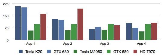
Non-Microsoft Direct3D GPGPU face-off: K20 vs 7970 vs GTX680 vs M2050 vs GTX580 from http://wili.cc/blog/gpgpu-faceoff.html

performance.png

K20 = GK110 (same chip design as NVIDIA Titan).

There's very difference between NVIDIA's OpenCL and CUDA.

cudaopencl.png

PS, Sony PS4 would not be using Microsoft's Direct3D stack.

App 1. Digital Hydraulics code is all about basic floating point arithmetics, both algebraic and transcendental. No dynamic branching, very little memory traffic.

App 2. Ambient Occlusion code is a very mixed load of floating point and integer arithmetics, dynamic branching, texture sampling and memory access. Despite the memory traffic, this is a very compute intensive kernel.

App 3. Running Sum code, in contrast to the above, is memory intensive. It shuffles data through at a high rate, not doing much calculations on it. It relies heavily on the on-chip L1 cache, though, so it's not a raw memory bandwidth test.

App 4. Geometry Sampling code is texture sampling intensive. It sweeps through geometry data in "waves", and stresses samplers, texture caches, and memory equally. It also has a high register usage and thus low occupancy.

-------------


Minus GPU's fix graphics function units, 7970 preforms well with complex GpGPU workloads. AMD needs to imporve GCN's non-compute hardware.

http://misterxmedia.livejournal.com's statement on VLIW is LOL

VLIW GPU 1 instruction represent : whole 64 operation ( you see the problem here, as very difficult for compiler to create this instruction , as per instruction has no dependency each other) - misterxmedia

VLIW is not like SIMD i.e. SIMD has single instruction with multiple data. SIMD is data level parallelism.

VLIW has multiple instructions with single corresponding data i.e. instruction level parallelism. http://en.wikipedia.org/wiki/Very_long_instruction_word :lol:

Avatar image for clyde46
clyde46

49061

Forum Posts

0

Wiki Points

0

Followers

Reviews: 1

User Lists: 0

#116 clyde46
Member since 2005 • 49061 Posts
Don't compare the 680 with anything in DirectCompute as Nvidia crippled it.
Avatar image for ronvalencia
ronvalencia

29612

Forum Posts

0

Wiki Points

0

Followers

Reviews: 1

User Lists: 0

#117 ronvalencia
Member since 2008 • 29612 Posts

[QUOTE="ronvalencia"]

Definition of POSSIBLE

1

a : being within the limits of ability, capacity, or realization

b : being what may be conceived, be done, or occur according to nature, custom, or manners

2

a : being something that may or may not occur lol.gif

b : being something that may or may not be true or actual lol.gif

----------

tormentos

In your small world it was possible...

How can it be possible for the xbox one to have a Volcanic Island GPU when every source say its GPU is GCN.?

Without GCN2 it was impossible that the xbox one include a Volcanic Island GPU.

"will have" != possible.

"must have" != possible.

http://oxforddictionaries.com/definition/english/possible

2. that may exist or happen, but that is not certain or probable:

http://www.merriam-webster.com/dictionary/possible

Definition of POSSIBLE

1

a : being within the limits of ability, capacity, or realization

b : being what may be conceived, be done, or occur according to nature, custom, or manners

2

a : being something that may or may not occur lol.gif

b : being something that may or may not be true or actual lol.gif

http://www.macmillandictionary.com/dictionary/british/possible

2. considered capable of happening, existing, being done, or being true, but not very likely possible (that): :lol:

-----------

You got problems with details.

Avatar image for AD216
AD216

1719

Forum Posts

0

Wiki Points

0

Followers

Reviews: 0

User Lists: 0

#118 AD216
Member since 2008 • 1719 Posts

why do i get on yo threads? they add nothing to this site

Avatar image for clyde46
clyde46

49061

Forum Posts

0

Wiki Points

0

Followers

Reviews: 1

User Lists: 0

#119 clyde46
Member since 2005 • 49061 Posts

why do i get on yo threads? they add nothing to this site

AD216
They do add to your post count though.
Avatar image for AD216
AD216

1719

Forum Posts

0

Wiki Points

0

Followers

Reviews: 0

User Lists: 0

#120 AD216
Member since 2008 • 1719 Posts
[QUOTE="AD216"]

why do i get on yo threads? they add nothing to this site

clyde46
They do add to your post count though.

lmao that's basically it. he's an obvious troll who sucks people in by making the most ridiculous statements possible.
Avatar image for menes777
menes777

2643

Forum Posts

0

Wiki Points

0

Followers

Reviews: 0

User Lists: 0

#121 menes777
Member since 2003 • 2643 Posts

[QUOTE="ronvalencia"]

[QUOTE="CallOfDutyRulez"]

:lol: Look at this dumb cow damage controlling.

No, that 5 billion transistor count is for the GPU ONLY confirmed by misterxmedia and mistercdream, both reliable insiders.

CallOfDutyRulez

GPU's register data storage, L1 cache, local data store, global cache and L2 cache are SRAM type memory.:lol:


Read http://news.xbox.com/2013/05/marc-whitten-and-major-nelson-discuss-xbox-one-architecture

5 billion's context is the same as Xbox 360's 500 million transistors (which includes 10MB eDRAM).


Due to the lack of GDDR5 memory, 32 MB ESRAM would be integral part of X1's GPU.

No, the 5 billion transistor is for the GPU ONLY. Get it through your dumb cow brain.

The eSRAM is not included in that figure.

No you're a dumbass, get it through your brain.

Avatar image for KungfuKitten
KungfuKitten

27389

Forum Posts

0

Wiki Points

0

Followers

Reviews: 42

User Lists: 0

#122 KungfuKitten
Member since 2006 • 27389 Posts

5 billion transistors.
What a waste of electricity.
Stop burning the trees!

Avatar image for ronvalencia
ronvalencia

29612

Forum Posts

0

Wiki Points

0

Followers

Reviews: 1

User Lists: 0

#123 ronvalencia
Member since 2008 • 29612 Posts

5 billion transistors.
What a waste of electricity.
Stop burning the trees!

KungfuKitten
I have 1.5 Kilowatt/hr solar cells on my roof.
Avatar image for Wasdie
Wasdie

53622

Forum Posts

0

Wiki Points

0

Followers

Reviews: 23

User Lists: 0

#124 Wasdie  Moderator
Member since 2003 • 53622 Posts

Enough is enough guys.