

https://twitter.com/XboxP3/status/1260681227071131648
EPIC has claimed RTX 2070 Super (entry-level TU104) running the same UE5 demo has "pretty good performance".
https://www.pcgamer.com/unreal-engine-5-tech-demo/
Would this demo run on my PC with a RTX 2070 Super? Yes, according to Libreri, and I should get "pretty good" performance.
Epic Games chief technical officer Kim Libreri.
-----
The last time a game with pixel density triangles has gimped AMD GPUs into oblivion.

On the PC, AMD used driver side intercept API calls to limit excessive tessellation from NVIDIA's Gameworks.
Vega 56/Vega 64/VII has four triangles input with four triangle output per clock cycle.
NAVI 10 has eight triangles input with four triangle output per clock cycle, hence blackface culling is working, but raw geometry power remains Vega GCN like.
PS5 renders UE5 demo at mostly 1440p and 30 fps.

For a given generation, AMD's memory access times are the same for DDR3 (A6-3650) and GDDR5 (HD 6850).
Intel memory controller's access times are lower, hence superior over AMD's.

From https://www.computer.org/csdl/journal/si/2019/08/08674801/18IluD0rWjS
GDDR5 and DDR4 have similar latency.
GDDR6 has lower latency when compared to GDDR5 (a claim made by Rambus).
https://www.rambus.com/blog_category/hbm-and-gddr6/
AI-specific hardware has been a catalyst for this tremendous growth, but there are always bottlenecks that must be addressed. A poll of the audience participants found that memory bandwidth was their #1 area for needed focus. Steve and Bill agreed and explored how HBM2E and GDDR6 memory could help advance AI/ML to the next level.
Steve discussed how HBM2E provides unsurpassed bandwidth and capacity, in a very compact footprint, that is a great fit for AI/ML training with deployments in heat- and space-constrained data centers. At the same time, the excellent performance and low latency of GDDR6 memory, built on time-tested manufacturing processes, make it an ideal choice for AI/ML inference which is increasingly implemented in powerful “IoT” devices such as ADAS in cars and trucks.
For Witcher 3, XBO rivals stock GTX 750.
Stock GTX 750 beats R7-250X/7770. https://www.techpowerup.com/review/nvidia-geforce-gtx-750-ti/25.html
Factor in NVIDIA's superior memory compression and effective physical memory bandwidth e.g.

Fury X has 512 GB/s raw memory bandwidth with 322 GB/s effective physical memory bandwidth and a small memory compression recovery.
----

Polaris memory compression has improvements for Tonga/Fury that recovers all the inefficiencies with the memory sub-system.
The kicker from Titan Pascal's effective memory bandwidth

NVIDIA made sure memory bandwidth is not a major bottleneck for their ex-flagship Titan X Pascal GPUs.
AMD Vega's memory compression is garbage since it couldn't recover inefficiencies with its memory subsystem.
GTX 1080 can take on Vega 64. The major problem with GTX 1080 is the lack of raw TFLOPS power which is solved with Turing RTX.
Turing has further memory compression improvements over Pascal.

NVIDIA's real-time memory compression is optimized for color and BCn compression
https://www.techpowerup.com/review/asus-radeon-rx-5700-xt-strix-oc/33.html

ASUS RX 5700 XT Strix has 2007 Mhz clock speed average, hence 10.275 TFLOPS
https://www.eurogamer.net/articles/digitalfoundry-2020-playstation-5-the-mark-cerny-tech-deep-dive
Cerny also stresses that power consumption and clock speeds don't have a linear relationship. Dropping frequency by 10 per cent reduces power consumption by around 27 per cent. "In general, a 10 per cent power reduction is just a few percent reduction in frequency," Cerny emphasises.
90% of CPU at 3.5Ghz = 3.15 Ghz, 806 GFLOPS.
or
90% of GPU at 2.23 Ghz = 2.01 Ghz, 9.248 TFLOPS <---- LOL, Mark Cerny, what are you doing? LOL,
Mark Cerny just confirmed 9.248 TFLOPS GPU from Github leak LOL.
Mark Cerny should NOT have stated: "Dropping frequency by 10 percent reduces power consumption by around 27 percent". LOL
Mark Cerny already stated a developer already found max GPU clock speed with a certain CPU load workload profile.
---------
Cow's 32 ROPS debate revisited.
RX 460 has 16 ROPS and it's approaching R9-270X (Pitcairn XT)

RX 460 has 14 CU (2.1 TFLOPS) with 112 GB/s memory bandwidth with Polaris DCC.
Applying Polaris DCC 1.4X on 112 GB/s yield 159 GB/s
R9-270X has 2.688 TFLOPS with 179.2 GB/s memory bandwidth
RX 460's 16 ROPS just wreaked cow's 32 ROPS argument.
https://vga-card-array.blogspot.com/2018/11/12-fresh-rx-560-vs-950.html


PC GCN 1.0 has two ACE units with a total of 16 queued context.
PC GCN 1.1 has up to eight ACE units with a total of 64 queued context.
Game console GCNs has an extra Graphics CP (Command Processor)

ATI's fusion concept is the genesis for AMD's GCN fusion with CPU capability

CPU and GPU are pointer copy capable which is not possible for PS3's "teh CELL" i.e. SPU is incapable to read CPU's pointers.


This is why Xbox 360's fusion model was the real CPU/GPU fusion.
IBM CELL's CPU and SPUs couldn't exchange pointers.
IBM CELL's SPUs couldn't exchange pointers with NVIDIA's RSX.
For NVIDIA camp, https://devblogs.nvidia.com/unified-memory-cuda-beginners/
https://www.eurogamer.net/articles/digitalfoundry-2020-inside-xbox-series-x-full-specs
RDNA 2 fully supports the latest DXR Tier 1.1 standard, and similar to the Turing RT core, it accelerates the creation of the so-called BVH structures required to accurately map ray traversal and intersections, tested against geometry
...
"Without hardware acceleration, this work could have been done in the shaders, but would have consumed over 13 TFLOPs alone," says Andrew Goossen. "For the Series X, this work is offloaded onto dedicated hardware and the shader can continue to run in parallel with full performance. In other words, Series X can effectively tap the equivalent of well over 25 TFLOPs of performance while ray tracing."
RDNA 2 has RT cores (accelerates BVH structures) which can continue to run in parallel with shader rasters (accelerates z-buffer structures) with full performance.
-------------------------
For comparison, Turing's RT cores.
TURING RT CORES At the heart of Turing’s hardware-based ray tracing acceleration is the new RT Core included in each SM. RT Cores accelerate Bounding Volume Hierarchy (BVH) traversal and ray/triangle intersection testing (ray casting) functions.
From https://www.eurogamer.net/articles/digitalfoundry-2020-inside-xbox-series-x-full-specs
but there was one startling takeaway - we were shown benchmark results that, on this two-week-old, unoptimised port, already deliver very, very similar performance to an RTX 2080.
https://youtu.be/oNZibJazWTo?t=726

51 / 39 = 1.30 or 30%
https://www.guru3d.com/articles_pages/gears_of_war_5_pc_graphics_performance_benchmark_review,6.html
Gears 5 with PC Ultra settings at 4K
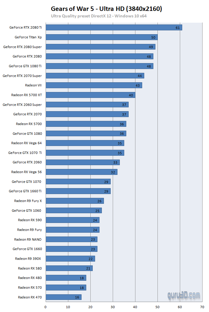
Scale RX 5700 XT's 9.66 TFLOPS** into XSX's 12.147 TFLOPS and it lands on RTX 2080 class level i.e. 50 fps
**Based from real-world average clock speed for RX 5700 XT from https://www.techpowerup.com/review/amd-radeon-rx-5700-xt/34.html
12.147 / 9.66 = 1.25745 or 25.745%, hence XSX GPU has ~25.75% extra TFLOPS over RX 5700 XT.
Gears 5's ranking follows

Apply 1.25 on RX 5700 XT's 122% and it would on land 152.5% which is between RTX 2080 and RTX 2080 Super.
--------------------
Against PS5, it's more than 18.21% difference when Sony added extra GPU TFLOPS on the same 448 GB/s memory bandwidth as RX 5700 and RX 5700 XT.
RX 5700 XT stock and RX 5700 XT factory overclock with the same 448 GB/s memory bandwidth are already showing diminishing returns relative to RX 5700's 7.7 TFLOPS.
https://www.techpowerup.com/review/asrock-radeon-rx-5700-xt-taichi-oc-plus/33.html
This RX 5700 XT Taich OC has 1996 Mhz average, hence 10.219 TFLOPS.
https://www.techpowerup.com/review/asrock-radeon-rx-5700-xt-taichi-oc-plus/27.html

For XSX's estimate, apply 1.25 on RX 5700 XT's 96% lands on 120% which is RTX 2080 level.
AMD needs to spec-up RX 5700 XT with GDDR6-15500 rated modules.
Zen 2 CPU's Infinity Fabric limitations ("sweet spot") according to AMD.

Dual-channel DDR4-3733 has 59.728 GB/s
Log in to comment