
At the bottom of that page you'll see that OptiX 1.0 was released Nov 3, 2009.
Year 2010 NVIDIA Design Garage Fermi launch demo
64-bit version handling bigger data
At the bottom of that page you'll see that OptiX 1.0 was released Nov 3, 2009.
Year 2010 NVIDIA Design Garage Fermi launch demo
64-bit version handling bigger data
https://www.tomshardware.com/news/amd-patents-hybrid-ray-tracing-solution,39761.html
AMD patent source link http://www.freepatentsonline.com/20190197761.pdf
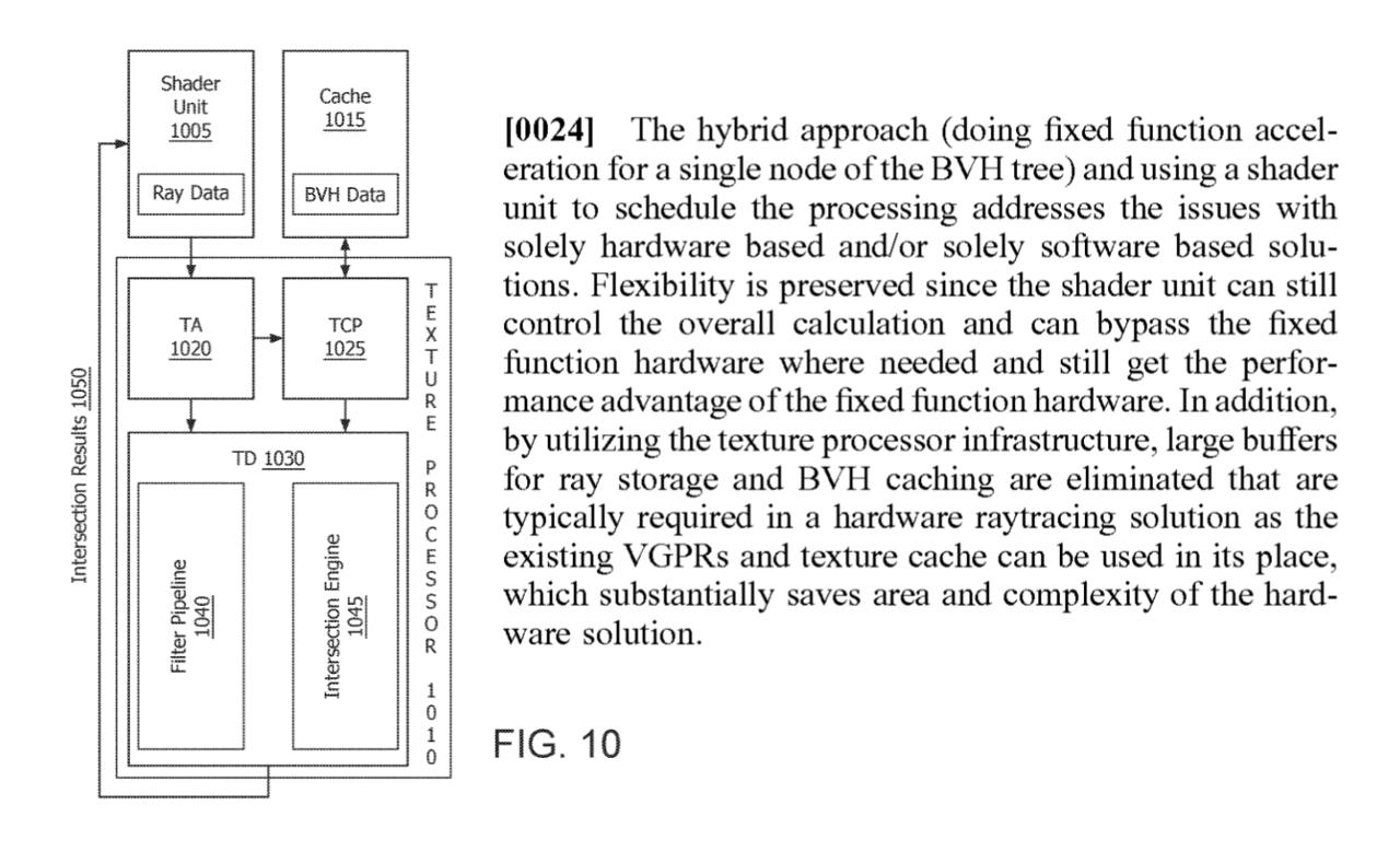
"Claim 19:. A texture processor comprising: a texture address unit connected to a shader; a texture cache connected to the texture address unit; a ray intersection engine connected to the texture address unit, the texture cache and the shader; wherein: the texture address unit is configured to: receive from the shader a texture instruction which includes at least a bounded volume hierarchy (BVH) node pointer and ray data; filter the texture instruction to obtain the ray data; fetch BVH node data from the texture cache based on the BVH node pointer, the ray intersection engine is configured to: receive the ray data and the BVH node data; perform ray-BVH node type intersection testing using the ray data and the BVH node data; and send intersection results based on the ray-BVH node type intersection testing via a texture data return path to the shader."
In the DETAILED DESCRIPTION section:
"A texture processor based ray tracing acceleration method and system are described herein. A fixed function BVH intersection testing and traversal (a common and expensive operation in ray tracers) logic is implemented on texture processors. This enables the performance and power efficiency of the ray tracing to be substantially improved without expanding high area and effort costs."
"In particular, a fixed function ray intersection engine is added in parallel to a texture filter pipeline in a texture processor. This enables the shader unit to issue a texture instruction which contains the ray data (ray origin and ray direction) and a pointer to the BVH node in the BVH tree. The texture processor can fetch the BVH node data from memory and supply both the data from the BVH node and the ray data to the fixed function ray intersection engine.
The ray intersection engine looks at the data for the BVH node and determines whether it needs to do ray-box intersection or ray-triangle intersection testing (Note 1).
The ray intersection engine configures its ALUs or compute units accordingly and passes the ray data and BVH node data through the configured internal ALUs or compute units to calculate the intersection results (Note 2).
Based on the results of the intersection testing, a state machine determines how the shader unit should advance its internal stack (traversal stack) and traverse the BVH tree. (Note 3)
The state machine can be fixed function or programmable. The intersection testing results and/or a list of node pointers which need to be traversed next (in the order they need to be traversed) are returned to the shader unit using the texture data return path. The shader unit reviews the results of the intersection and the indications received to decide how to traverse to the next node in the BVH tree."
AMD's year 2017 RT patent doesn't completely detach shader resource with tree transversal workloads.
NAVI CU has increased texture filter processor width by 2X over GCN CU. AMD is preparing TMUs to be burden down with additional workload workloads.
TA = Texture Address Unit. Read/write instructions from compute shaders. Shaders could contain embeded data playload beside shader instructions.
TCP = Texture Cache Processor Unit, read/write data from on-chip cache.
It's logical to conclude placing "Interection Engine" in the TMU.
---
Note 1. Almost NVIDIA RT core equalvent. AMD recycled TCP unit for the fetch operation. NVIDIA RT has it's own fetch operation unit.
Deciding (branching) between ray-box intersection or ray-triangle intersection testing is similar to NVIDIA RT's 1st stage.
NVIDIA RT's can advance it's search tree node via independent loops and repeated fetch operations.
Note 2. From ray intersection engine, AMD is not sure between internal ALU or compute unit to calculate the intersection results.
Note 3. Advancing it's search tree node via shaders.
NVIDIA RT's can advance it's search tree node via independent loops and repeated fetch operations.
NVIDIA Turing RTX reference

https://wccftech.com/gran-turismo-polyphony-raytracing/
Gran Turismo developer Polyphony Digital revealed they’ve created their own in-house real-time ray tracing tech
This in-house "ray tracing" indicates non-DXR/RTX bounding volume hierarchy ray-tracing method.
Polyphony Digital's "raytracing" is based on path-tracing which are one of "cheap rays" methods
At SIGGRAPH Asia 2018, Polyphony Digital confirmed that they were experimenting with real-time ray tracing, developing their own path tracing solution to offer accurate reflections that offer a notable graphical leap over the pre-baked reflections that are used in their recent games.
Sony is again playing lose with raytracing from "cheap rays" methods.
This is Sony's direct response to Microsoft DXR/NVIDIA RTX Turing marketing.
From https://www.anandtech.com/show/14579/all-ryzen-qa-with-amd-ceo-dr-lisa-su
David Wang, AMD: We started RDNA before the Sony engagement. I think RDNA is revolutionary, and it is very flexible in terms of being able to be customized for different types of workloads.
NAVI was designed before the Sony engagement, hence debunking
https://segmentnext.com/2018/06/13/amd-navi-sony-playstation-5/
https://www.pcgamesn.com/amd/navi-sony-ps5-hardware-exclusivity

HC-14 GDDR6 comes from Samsung.
It's GDDR6-14000.

320 bit GDDR6-14000 ???? LOL
About twice the memory bandwidth over Xbox Scorpio.
Alright broke out the measurement taping and found out some things about Navi and the Anaconda in terms of sizes on 7nm.
5700:
GDDR6 phy controller: 4.5mm x 8
Dual CU: 3.37mm x 20
4 ROP cluster: .55mm x 16
L1+L2+ACE+Gemotry processor+empty buffer spaces + etc: 139mm
Now Anaconda:
A rougher estimate using the 12x14mm GDDR6 chips next to the SOC.
370mm-390mm.
It's a bit bigger than the 1X SOC for sure.
If we use the figure of 380mm,
75mm for CPU
45mm for 10 GDDR6 controllers
8.8mm for ROPs
140mm for buses, caches, ACE, geometry processors, shape etc. I might be over estimating this part as the 5700 seems to have lots of "empty" areas.
We have ~110mm left for CUs + RT hardware. There is enough there for ~30 dual CUs and RT extensions.
Conclusion:
The Anaconda SOC is around the minimum size you need to fit the maximum Navi GPU and Zen2 cores.
I expect Anaconda to have a minimum of 48 CUs if the secret sauce is extra heavy or 60CUs if the sauce is light.

>24mm x >16mm = >384 mm2.
Scarlet is Xbox Anaconda follow on from Xbox Scorpio.
----------

-------------------
http://raytracey.blogspot.com/2018/07/accelerating-path-tracing-by-using-bvh.html
Advantages of using the BVH itself as multi-resolution LOD geometry representation:
(Note: AFAIK low level access to the acceleration structure is not provided by API's like OptiX/RTX and DXR, this has to be written in CUDA, ISPC or OpenCL)
-----------------------
https://semiwiki.com/semiconductor-manufacturers/samsung-foundry/7926-samsung-vs-tsmc-7nm-update/

In terms of silicon maturity, X1X is based on Vega
Vega 64 LC has 295 watts for 13 TFLOPS boost clock or Vega 64 LC's 11.5 TFLOPS base clock
X1X GPU has ~150 watts for 6 TFLOPS base clock
Vega 64's TFLOPS vs TDP scales from X1X GPU's logic design maturity!
RX-580's 6 TFLOPS has 185 watt. Polaris 20 has inferior TFLOPS per watts when compared to X1X GPU and Vega 64
Polaris 10/20 can't scale to Vega 64's TFLOPS vs TDP ratios.

PS4 Pro GPU's 2.3X gain over 28 nm GCN is based on 1st gen Polaris electron leakage mitigation maturity.
--------
Polaris 30 RX-590's (225 watts TDP / 36 CU) scaled to 64 CU = 400 watts. Meanwhile Vega 64 has 295 watts TDP.
RX-590's 1545 Mhz has similar boost clock speed to Vega 64's 1536 Mhz.
AMD's perf/watts road map is real.
https://www.tomshardware.com/reviews/amd-radeon-rx-580-review,5020-6.html
RX-580's actual typical gaming power consumption is 209 watts, hence it overshot AMD's 185 watts TDP target.
X1X typical gaming power consumption for the entire machine is about 172 watts. https://www.anandtech.com/show/11992/the-xbox-one-x-review/6 hence the GPU is somewhere 145 watts where CPU has 20 watts + 2.5 inch HDD has 2.5 watts + cut-down South Bridge has ~2.5 watts.
https://www.tomshardware.com/reviews/amd-radeon-rx-480-polaris-10,4616-9.html
RX 480's gaming has 164 watts power consumption which overshot AMD's 150 watts TDP target. PS4 Pro GPU was reduce to 911 Mhz to budget for CPU+2.5 HDD+Optical drive+controller.
X1X's perf/watt against PS4 is about 3.2 which is about Vega's perf/watt
PS4 Pro's perf/watt against PS4 is about 2.3 which is about 1st gen Polaris's perf/watt
X1X has Variable Shading Rate like feature. https://www.eurogamer.net/articles/digitalfoundry-2017-the-scorpio-engine-in-depth
Andrew Goossen tells us that the GPU supports extensions that allow depth and ID buffers to be efficiently rendered at full native resolution, while colour buffers can be rendered at half resolution with full pixel shader efficiency. Based on conversations last year with Mark Cerny, there is some commonality in approach here with some of the aspects of PlayStation 4 Pro's design, but we can expect some variation in customisations - despite both working with AMD, we're reliably informed that neither Sony or Microsoft are at all aware of each other's designs before they are publicly unveiled.
Depth buffer deals with geometry render buffer
https://developer.nvidia.com/vrworks/graphics/variablerateshading
GCN

RDNA

NAVI's cache design follows Ryzen Zen v2 instead of Vega's cache design.
https://hexus.net/tech/news/graphics/131555-the-architecture-behind-amds-rdna-navi-gpus/
Looking at caching, Radeon takes a leaf from the Ryzen playbook and adds dedicated L1 cache and doubles the load bandwidth from the nearest cache to the ALUs. The purpose here is to reduce the cache access latency at every level, and that means an improvement in effective bandwidth because the requested data remains in caches rather than having to be pulled from slower framebuffer memory.
Microsoft's "hardware accelerated" ray-tracing confirmation will consume additional transistors on top of baseline NAVI GPU.


Microsoft's "hardware accelerated" ray-tracing confirmation indirectly indicates 7nm+ process node.
Next gen NAVI ~= RDNA 2
According to AMD, RDNA 2 to be released before year 2021, hence RDNA 2's product release is somewhere in year 2020.
https://www.techspot.com/news/80237-tsmc-7nm-production-improves-performance-10.html
N7+ has identical yield rates to N7 and will steadily improve, while also offering a 20% increase to transistor density. There’s also a 10% performance uplift or 15% power efficiency increase. AMD will take advantage of the former in their fourth-gen Ryzen which they’ve confirmed to use TSMC’s 7nm+
------------
The original news article comes from https://www.wired.com/story/exclusive-sony-next-gen-console/ DF is not the original news article.
The AMD chip also includes a custom unit for 3D audio that Cerny thinks will redefine what sound can do in a videogame. “As a gamer,” he says, “it's been a little bit of a frustration that audio did not change too much between PlayStation 3 and PlayStation 4. With the next console the dream is to show how dramatically different the audio experience can be when we apply significant amounts of hardware horsepower to it.”
The existing Radeon Rays 3.0 can be used with True-Audio Next (TAN)
https://gpuopen.com/gaming-product/true-audio-next/
The TAN library may be used in conjunction with Radeon Rays as foundational accelerated algorithms for a complete physics-based audio solution
Sony is on record claiming cheap rays as ray-tracing.
https://www.guerrilla-games.com/read/killzone-shadow-fall-creating-art-tools-for-a-new-generation
it describes light rendering systems used in a new 3D engine built from the ground up for upcoming PlayStation 4 hardware. A novel real-time lighting model simulating physically accurate Area Lights will be introduced, as well as hybrid- raytraced/image based reflection system
Meanwhile, EA DICE separated cheap rays from hierarchical ray-tracing e.g. bounding volume hierarchy (BVH) on NVIDIA RTX hardware and Microsoft's DXR API

From year 2015, EA DICE already hinted Turing RTX's two accelerated points.
1. Hierarchical
2. Intersection
---------------
https://twitter.com/albertpenello/status/1140693832821923841
IMO I would not place any faith in Dev Kit specs this early - chips aren't even close to ready. First Scorpio bring-up was 12/16 and real dev kits went out in March 2017. X1 and PS4 even later.
— Albert Penello (@albertpenello) June 17, 2019
We sent out Mac's for X360 dev kits. Dev kits mean very little at this point TBH.
https://twitter.com/noobde/status/1142052141365960705
Xbox Scarlet is more powerful than PS5.
— Ed Boon (@noobde) June 21, 2019
PS5 is more powerful than Xbox Scarlet.
How? HOW can anyone confidently make either statement without having WORKED on the FINAL hardware for each?

https://www.techcenturion.com/7nm-10nm-14nm-fabrication
Different companies markets their silicon density differently.
Intel's 10 nm is effectively TSMC's 7nm+ on apples to apples density comparison.
Claim:
GPU chips - Fair enough. Nvidia and AMD clearly lead in this category. Although both the Nvidia and AMD GPU divisions are founded and led by Asian immigrants.
US is a nation of migrants. US is consistent with helping/protecting Republic of China (located in Taiwan) since pre-WW2 to this day with a special defence agreement between US and Taiwan. US trade blockaded Imperial Japan to support Republic of China before WW2.
https://en.wikipedia.org/wiki/Nvidia#Founders_and_initial_investment
2 of 3 NVIDIA's co-founders are "white". NVIDIA's founding was banked rolled by https://en.wikipedia.org/wiki/Sequoia_Capital Sequoia was founded by "white" Don Valentine
Three people co-founded Nvidia in April 1993:[11][12]
Chris Malachowsky worked with HP and Sun.
In the early 1990s, Commodore was working with HP on PA-RISC based 3D chipset. HP fabricated Commodore's Amiga chipsets like AGA's Lisa chip (display chip).
https://en.wikipedia.org/wiki/Amiga_Hombre_chipset
According to Dr. Ed Hepler, Hombre was to be fabricated in 0.6 µm 3-level metal CMOS with the help of Hewlett-Packard. HP had fabricated the AGA Lisa chip and collaborated in the design of the AAA chipset.
Amiga Hombre was early 1990s "Xbox" which can run MS's Windows NT 3.1 with OpenGL (licensed from SGI).
The original plan for the Hombre-based computer system was to have Windows NT compatibility, with native AmigaOS recompiled for the new big-endian CPU to run legacy 68kAmiga software through emulation. Commodore chose the PA-7150 microprocessor over the MIPSR3000 microprocessor and first generation embedded PowerPC microprocessors, mainly because these low-cost microprocessors were unqualified to run Windows NT. This wasn't the case for the 64-bitMIPSR4200, but it was rejected for its high price at the time.
Microsoft developed their Xbox when it run out of game console hardware partners.
US EPA killed Commodore.
------
Claim:
Space industry - 4 out of the top 5 countries with the highest space research & exploration funding are Asian.
https://www.alphr.com/space/1005737/how-much-do-governments-spend-on-space-science

US located Space X leads the rocket tech innovation which has beaten every government run rocket programs.
Claim:
Most of Russia's land is in Asia, and its space launch facilities are in Asia. Russia is never called "Western" but has always been "the East". Still not relevant, US has a clear lead here. Anyone thinking the rest of the world isn't following their lead is just disingenuous.
Russia's current civilisation is based on Eastern "Holy" Roman empire's Christian Orthodox branch.
US and majority of EU civilisation is based on Western "Holy" Roman empire's Catholic/Protestant Christian branch.
Read https://en.wikipedia.org/wiki/East%E2%80%93West_Schism
Claim:
Fact is both Russia's and US space program were kickstarted by German/Nazi talent.
Reminder, English and German languages are part of Germanic family. Read https://en.wikipedia.org/wiki/Germanic_languages
Claim:
Automobile industry - 7 out of the top 10 best-ranked quality car brands are Asian, including #1 (Lexus). Again volume.
There are multiple Toyota factories in the US. https://en.wikipedia.org/wiki/List_of_Toyota_manufacturing_facilities#United_States including very popular Camry and Corolla models.
Claim:
German automobiles are more luxurious, have better quality and more sought after.
German automobiles like VW was caught cheating against US EPA's rules.
Tesla is leading the EV race and Giga-Factory is create near a Nevada Lithium mine. Unlike EU, North American continent is rich with raw metals and oil.

nVIDIA for the win with AI vehicle driving which has beaten both Japanese and German AI software/hardware developments.
Claim:
Multimedia formats - The current AVC and AAC standards were set by Japanese companies, when they created the Blu-ray format.
https://en.wikipedia.org/wiki/Advanced_Audio_Coding
| Developed by | Bell Labs, Fraunhofer Institute, Dolby Labs, Sony and Nokia |
|---|
US: Bell Labs
EU(germany): Fraunhofer Institute
US: Dolby Labs
JP: Sony
EU(Finland): Nokia
https://en.wikipedia.org/wiki/H.264/MPEG-4_AVC
H.264 was developed by the ITU-TVideo Coding Experts Group (VCEG) together with the ISO/IEC JTC1Moving Picture Experts Group (MPEG)
H.264 is protected by patents owned by various parties. A license covering most (but not all) patents essential to H.264 is administered by patent poolMPEG LA
https://en.wikipedia.org/wiki/MPEG_LA
That ultimately led to a group of eight MPEG-2 patent owners—Fujitsu, Panasonic, Sony, Mitsubishi, Scientific Atlanta, Columbia University, Philips and General Instrument—along with CableLabs and certain individuals, to form MPEG LA, which in turn created the first modern-day patent pool as a solution.
4 companies: Japan
4 companies (including Columbia University): US
1 company: EU
RX 580 has 1257 Mhz base clock (5.8 TFLOPS) with 1340 Mhz boost clock (6.1 TFLOPS, ~185 watts). X1X GPU has 1172 Mhz base clock without boost mode, hence X1X GPU has 93 percent of RX-580's base clock speed. Microsoft added extra 2MB render cache, 4 additional CUs and auto-under-volting smart VRM to deliver 6 TFLOPS FP32 GPU at lower power when compared to AMD's 6 TFLOPS RX 580 with 185 watts.
MS's X1X vs RX-580 basic parameters
Sony's PS4 Pro vs RX-480 basic parameters
MS has beaten Sony on rivalling the basic TFLOPS power from PC desktop's RX-580 while X1X GPU consumes less power when compared to AMD's RX-580 6 TFLOPS 185 watts configuration.
Facts for 16 nm era AMD GPUs: MS has shown to have superior electrical engineering skills (smart VRM design) over AMD's and Sony's electrical engineering skills.
Vega II's dumb VRM design shows AMD's lazy VRM craftsmanship as shown from this example https://www.reddit.com/r/Amd/comments/ao43xl/radeon_vii_insanely_overvolted_undervolting/
If Vega II has X1X's smart VRM design, this end user beta testing complaints would be less.
During Xbox 360's design, Surface Team did NOT exist, hence your Xbox 360 argument is a red herring.
Any argument on forcing Phil to claim the "most powerful console" argument without knowing PS5 is flawed.
Phil's response against "MS need to confirm they have the most powerful console" argument shows Microsoft monitors gaming forums.
The "MS need to confirm they have the most powerful console" argument is flawed since MS doesn't know about Sony's PS5 while MS can control statements about it's console specifications, hence hardware accelerated ray-tracing official claim.
Sony can control statements about it's console specifications which hasn't officially confirmed hardware accelerated ray-tracing.
Having smart VRM design is a matter better being lower than PC's RX-5700 XT AE or rivalling it.
Sony has revealed 8 core Zen v2 CPU for PS5.
---
AMD has revealed NAVI RX 5000 GPU series for PS5.
RX 5700 has similar chip area size to RX-480 "Polaris" and 7870 "Pitcairn" GPUs which are baseline GPU design for PS4 Pro and PS4 respectively.
GPU chip area size list
NVIDIA RSX = 258 mm2 for PS3
AMD RX-480 "Polaris" = 232 mm2 for PS4
AMD 7870 "Pitcairn" = 212 mm2 for PS4 Pro
AMD RX 5700 "NAVI ???" = 222.5mm2 (see reference note 1)
1. https://wccftech.com/amd-navi-rx-5700-is-only-the-mid-range-brings-rtx-2070-performance-at-half-the-die-size/
https://www.techpowerup.com/gpu-specs/geforce-rtx-2070.c3252
RTX 2070's 445 mm2 / 2 = 222.5 mm2
Sony is consistent with GPU selection chip area size.
PS5's GPU count be slightly larger due to semi-custom IP blocks from the next GPU design.
Sony mentions 8K which refers to HDMI 2.1's main feature. HDMI 2.1 also comes with AMD's FreeSync, hence locked 60 hz is not required.
---
Sony mentions ray-tracing with audio feature for PS5 which corresponds to AMD's Radeon Rays 3.0 "BHV search" enhancements with TrueAudio Next. https://gpuopen.com/gaming-product/true-audio-next/
The TAN library may be used in conjunction with Radeon Rays as foundational accelerated algorithms for a complete physics-based audio solution.
8 core Zen 2 chiplet size is about 70 mm2 https://www.reddit.com/r/Amd/comments/9uskmh/zen_2_die_size/
PS5 doesn't need desktop Zen v2 PC's IO north-bridge chip.
PS5: 70 mm2 + 223 mm2 = 293 mm2 for AMD's main GPU and CPU IP blocks covered.
PS4 APU total area size = 348 mm2
PS4 Pro APU total area size = 321 mm2
Sony has a reasonable chip area budget for semi-custom designs e.g. 55 mm2 chip area for custom work e.g. ray-tracing accelerator or slightly larger NAVI GPU.
---
Xbox Scorpio APU has 359 mm2 chip area size with larger GPU in the 285 mm2 range.
----
Both Vega II and Zen v2 supports Infinity Fabric interconnects hence CPU can directly connect to the GPU. One could assumes NAVI also supports Infinity Fabric interconnects.
GPU already has memory controllers.
https://www.theinquirer.net/inquirer/news/3075196/amd-cray-supercomputer
In AMD/Cray's supercomputer, Zen CPU is connected to Vega II GPU via Infinity Fabric interconnects
Ungaro continued: "The new accelerator-centric compute blades will support a 4:1 GPU to CPU ratio with high-speed AMD Infinity Fabric links and coherent memory between them within the node.
Raven Ridge APU's CPU and GPU are also connected by Infinity Fabric links.
Small north-bridge I/O would be needed for any south-bridge functions and north-bridge driven storage solutions.
Log in to comment