Both CPUs and GPUs equally benefit from semiconductor technology improvements, but on top of that the CPU can still significantly increase the compute density while the GPU can not. Therefore is said that the GPU is at the mercy of semiconductor technology improvements, while the CPU has more possibilities to increase performance.
The GpGPU has a very high instruction count per cycle and can be increased via clock speed. For this to happen, AMD would need to shift thier GPU designs to GoFlo fabs or TSMC improves thier fab tech.
Exactly. And because register files are less dense than caches this takes up a considerable amount of die space. And it's getting worse. Complex HPC applications need a true stack for storing function arguments.
On die space usage, it depends on the skills of the engineers.
Intel Larrabee is over 600 mm^2 at 45 nm and ~1.7 billion transistors.
AMD Radeon HD 4870, 263mm^2 at 55 nm and 956 million transistors.
AMD Radeon HD 5870, 334 mm^ 2 at 40 nm and 2.15 billion transistors.
AMD Radeon HD 6870,225 mm^2 at 40nm and 1.7 billion transistors.
Even if we normalise the AMD Radeon HD part to 45nm, the AMD Radeon HD 5870 is still smaller.
Also, AMD Radeon HD 5870's die size is smaller than NV Geforce GTX460 at the same 40nm process.
For instance the GF100 only has 1024 32-bit registers per scalar core. This may seem like a lot at first but note that they are shared by many strands to hide latency. And with RAM access latencies of around 600 clock cycles it's clear that this register file barely suffices and caches are needed to keep the number of RAM accesses down. It works out alright for graphics, but most HPC applications are a lot more demanding.
GF100 is connected to faster GDDR5 memory. Unlike DDR2 SDRAM's uni-directional signal strobe, GDDR3 use bi-directional signal strobe i.e. better write and read ratios. DDR3 SDRAM follows DDR2 SDRAM when it comes signal strobe.
CPUs used in HPC systems typically have around 12 MB of cache. The performance would plummet with smaller caches. So GPUs need similar amounts to become capable of running anywhere near the same range of applications. In conclusion it's really difficult to prevent today's GPUs from stalling a lot for HPC applications, and they'll need to sacrifice compute density to increase efficiency.
GPUs will just increase thier register and thread count e.g.AMD Bart.AMD Cayman is the last 40nm TSMC fab part before switching to 28nm.
Which illustrates the point that the compute density drops fast when you add things to make the GPU capable of more generic computing, on an affordably sized chip.
AMD sais Llano will offer 500 GFLOPS. That's nowhere near the 3 TFLOPS number you've been touting about earlier, and much closer to the several hundred GFLOPS CPUs could offer in the near future. In fact it would only take a 6-core 3 GHz CPU with two 256-bit wide FMA units to achieve 576 GFLOPS. CPUs like that will only appear about a year after Llano, but as you can see the gap is closing pretty rapidly and it makes a lot of sense to consider fully unifying them.
The mobile Llano CGPU part consumes around 20 to 59 watts. It's lower than my Core i7-740M QC+AMD 5730M's 71 watt combo.
Llano could change btw i.e. switch from VLIW5 to Cayman's VLIW4 uArch.
It's not that big of a mess. Sure there are some oddball legacy instructions, but the majority has a nicely structured encoding format. The die area spent on x86 decoding is only a few percent, and actuall shrinks every generation. It also hasn't stopped Intel from achieving TFLOPS performance on early Larrabee prototypes.
On transistor count vs performance vs die size, Larrabee is a joke.
GPUs have a bigger problem. Their instructions are not compacted so they need more storage. And there's still a hard limit on the kernel size. Also, to improve efficiency they need to be capable of running more kernels in parallel. This again requires additional instruction storage. So once again the only solution is to evolve toward a CPU architecture.
...
No problem with AMD's Radeon HD logic packing engineering skills. Both NVIDIA and Intel just makes large/bloated cores.
SGEMM is merely a synthetic benchmark. It's not much of an indication of practical performance of the entire system. There are plenty of things the CPU truely excels at, but are not showing you the big picture either.
As stated above, AMD presents a balance view on this issue.
Let me remind you again that AMD's GPUs have almost twice the GFLOPS ratings as NVIDIA's GPUs, but their results in games are comparable.
As I stated eariler, there are other bottlenecks in the design e.g.raster rendering issue.
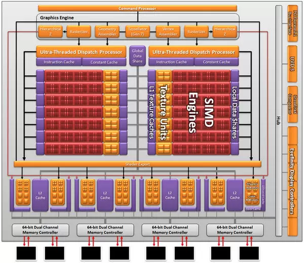
Unlike AMD Cypress and RV770, notice why AMD's Bart includes two Ultra-Threaded Dispach processor front-end blocks.


Log in to comment